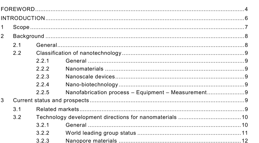
IEC TR 62834-2013 pdf IEC nanoelectronics standardization roadmap

The largest part of the market of mass production equipment is in nanostructure thin film materials, as well as tools, moulds and various mechanic parts. At present, equipment companies operating worlwdie (e.g. Kobe, Cemecon, Balzers, Huazer 2 ) have developed their equipment and handled materials, processes and patents collectively. The market of nanocomposite materials is led by polymer matrix nanocomposites, with a world market size of about 5 billion – 7 billion US dollars in 2009. The market of ceramic nanocomposite materials was about 2,5 billion US dollars after 201 0. The market has shown a consistent growth trend due to continuous growth in several ten gigabyte (GB) high capacity flash memory and DRAM components. Given the vague overlapping area of existing semiconductor and nanotechnology markets, it is important to analyse characteristics, to standardize the modelling and design methodology and to obtain circuit IP based on nanoelectronic devices to address the nanotechnology market. III-V compound semiconductors including nitride-based nanostructures will be used for light- emitting diodes (LEDs), and their scope of application continues to expand, including portable appliances, LCD (liquid chrystal display) backlight, automobile lighting. The most active area is the LED market, and many players are striving to launch into the general lighting market. The LED lighting industry is expected to replace almost all lighting areas such as traffic signals, construction and automobiles as well as LCD backlighting and general lighting. In addition, development and commercialization of quantum dot light receiving devices and infrared devices are expected to bring about a revolution in the area of image sensors. Solar energy is an area that has seen double-digit growth rates due to worldwide energy issues. The flexible electronic device market is expected to grow rapidly from 1 6 million US dollars seen in 2008 to 1 ,31 4 million US dollars in 201 3.
Technology development of nanocomposite materials in the USA is conducted in the “Nanostructured material by design” program of the National Nanotechnology Initiate (NNI) announced in 2000. The U.S. Department of Defense is devoted to the development of high strength-to-weight materials, the Department of Energy, to the development of wear-resistant and corrosion-resistant ceramic nanocomposite materials, and NASA, devoted to the development of nanocomposite materials with high strength and low specific gravity (light weight) for space shuttles. National Aeronautics and Space Administration (NASA) has developed ultra-light carbon nanocomposite materials with high heat resistance to replace body parts. These were manufactured with existing carbon textile and fiberglass for improved heat resistance performance and fuel savings for space shuttles. NASA attempted to dominate the world market in the area of new concept aerospace technology to be expanded in the future.
- ISO IEC 27050-4-2021 pdf Information technology — Electronic discovery — Part 4: Technical readiness
- ISO IEC 27036-1-2021 pdf Cybersecurity — Supplier relationships — Part 1: Overview and concepts
- ISO IEC 27013-2021 pdf Information security, cybersecurity and privacy protection — Guidance on the integrated implementation of ISO/IEC 27001 and ISO/IEC 20000-1
- ISO IEC 26580-2021 pdf Software and systems engineering — Methods and tools for the feature- based approach to software and systems product line engineering
- ISO IEC 24735-2021 pdf Information technology — Office equipment — Method for measuring digital copying productivity
- ISO IEC 24711-2021 pdf Information technology — Office equipment — Method for the determination of ink cartridge yield for colour inkjet printers and multi- function devices that contain printer components
- ISO IEC 23544-2021 pdf Information Technology — Data centres — Application Platform Energy Effectiveness (APEE)
- ISO IEC 23510-2021 pdf Information technology — 3D printing and scanning — Framework for an Additive Manufacturing Service Platform (AMSP)
- ISO IEC 23127-1-2021 pdf Information technology — Learning, education, and training — Metadata for facilitators of online learning — Part 1: Framework
- ISO IEC 23126-2021 pdf Information technology for learning, education and training — Ubiquitous learning resource organization and description framework
- IEC 62488-3-2021 pdf Power line communication systems for power utility applications – Part 3: Digital Power Line Carrier (DPLC) Terminals and hybrid ADPLC Terminals
- IEC 62973-4-2021 pdf Railway applications – Rolling stock – Batteries for auxiliary power supply systems – Part 4: Secondary sealed nickel-metal hydride batteries
- IEC 61156-8-2013 pdf Multicore and symmetrical pair/quad cables for digital communications – Part 8: Symmetrical pair/quad cables with transmission characteristics up to 1 200 MHz – Work area wiring – Sectional specification
- ISO IEC 27050-4-2021 pdf Information technology — Electronic discovery — Part 4: Technical readiness
- IEC 62148-21-2021 pdf Fibre optic active components and devices – Package and interface standards – Part 21: Design guidelines of electrical interface of PIC packages using silicon fine-pitch ball grid array (S-FBGA) and silicon fine-pitch land grid array (S‑FLGA)
- BS ISO IEC 15420-2009 pdf Information technology一 Automatic identification and data capture techniques EAN/UPC bar code symbology specification
- BS IEC 60860-2014 pdf Radiation protection instrumentation一 Warning equipment for criticality accidents
- BS ISO IEC 19762.5-2008 pdf Information technology一 Automatic identification and data capture (AIDC) techniques – Harmonized vocabulary Part 5: Locating systems
- ISO IEC 24735-2021 pdf Information technology — Office equipment — Method for measuring digital copying productivity
- ISO IEC 24711-2021 pdf Information technology — Office equipment — Method for the determination of ink cartridge yield for colour inkjet printers and multi- function devices that contain printer components